Laser systems the revolution in PCB manufacturing
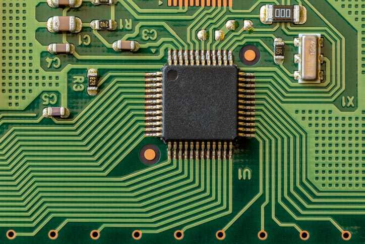
Virtually all electronic devices contain one or more printed circuit boards. They serve as an insulating and connective support element for the circuitry inside mobile phones, smart watches, computers, printers and robots, to name just a few examples.
Printed circuit boards, also known simply as circuit boards or boards, are commonly referred to as PCBs for short. The various elements within the electronic circuitry, such as integrated circuits (ICs), transistors, resistors and capacitors, are mounted on the PCB and simultaneously connected to it electrically via conductive paths made of copper. Incidentally, the modern PCB was developed by a German called Fritz Stahl in the 1950s.
As boards became increasingly small and complex in their layout, touch-free and contact-free laser systems began to revolutionise their processing. By the time the 5G standard for mobile technologies was introduced in 2020, lasers were already well established at the forefront of material processing technologies in the PCB industry.
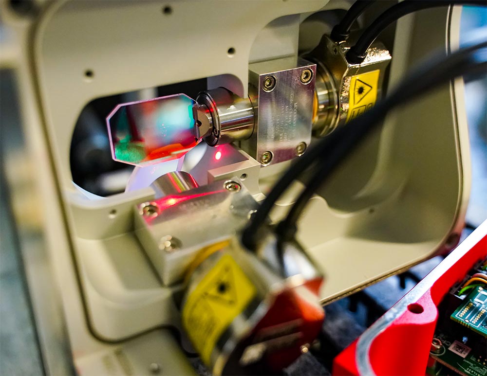
Source ASYS marking and reading stations
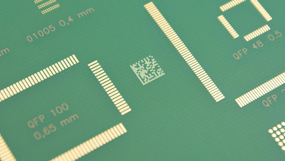
Markings as tiny as a grain of sand
PCBs are branded or marked to facilitate traceability. The industry often uses barcodes or 2D codes in various formats. Due to the ever-increasing packing densities on PCBs, the amount of space available for marking is diminishing all the time. Currently, standard PCBs have code sizes ranging from 5 mil to 7.5 mil. However, the trend is towards ever-decreasing miniature code sizes of just 3 mil. To fully appreciate how small this is, consider for a moment that 1 mil corresponds to one-thousandth of an inch, or just 0.025 mm. These tiny dimensions are invisible to the naked eye.
Most PCBs are marked using CO2 lasers. This process pro- duces a colour change in the (usually green) solder resist covering the surface of the PCB, which serves to protect the board and improve its electrical properties. However, CO2 lasers reach their physical limits at a pixel size of 75 μm, and so other solutions have to be found.
One alternative is presented by fibre lasers. Rather than changing the colour of the solder resist, these ablate the surface right the way through to the underlying copper layer. Laser beams in the green (532 nm) and blue (450 nm) wavelength range are another option. The solder resist absorbs these very well and their short wavelengths enable very small spot diameters, so that code sizes of less than 3 mil no longer present a problem.
With low laser power levels of just 6 W at 450 nm and thanks to scanner technology, these lasers can mark codes that are easily read. In most cases, the code is read immediately after laser marking, either on-axis with the scanner or off-axis – simply and accurately. If the marking on the PCB panel (also known as a multiblock) is faulty, the scrap component can be easily eliminated following depaneling.
In electrical interconnection technology, a panel is a complete printed circuit board that consists of individual printed circuit boards and is not yet separated.
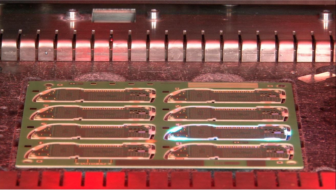
Laser depaneling no one cuts more precisely and cleanly
Laser depaneling is one of the most innovative processes used to separate single PCBs from a PCB panel. During depaneling, the PCBs are usually separated by means of a focussed laser beam that removes the material layer by layer in a process known as ablation. As a rule, the laser does not separate the PCBs entirely from the panel. Instead, most of the laser cutting is done at the links that connect the single PCBs with one another.
Conventional mechanical processes have clear drawbacks when compared to lasers. In addition to tool wear and mechanical component stress, they also work much less cleanly than lasers. At worst, this can result in contamination and breakage of the entire PCB panel or of the circuits and soldered joints.
Lasers remove the links between the PCB by means of ablation, as described above. These connecting points may need to be targeted 50 to 100 times with the laser, depending on the thickness of the panel. To meet the increased demand for precision, the lasers in use today offer spot diameters of no more than 25 μm.
Laser cutting technologies offer significant benefits in this context, as the processing is touch-free and shape cutting of the PCBs is freely programmable. These days, the trend is towards ever-smaller PCB panels, which also means increasingly thin materials.
Spoilt for choice different PCB types
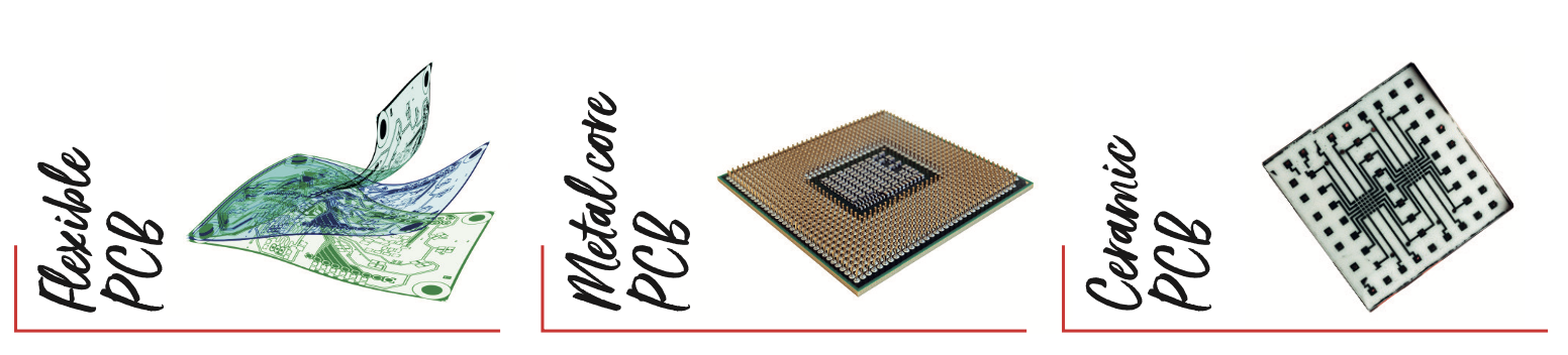
Various types of PCBs exist – rigid, flexible, metallic and ceramic. Flexible PCBs are used in cases where the finished product can be manipulated or folded, as is the case with medical devices like hearing aids. Meanwhile, metallic PCBs are used in connection with high voltage, while the ceramic type is suitable for use in conjunction with high electrical currents, e.g. in sensor applications and electric cars. Flexible PCBs made of polyimide and those with a metal core are removed entirely by laser. In contrast, ceramic PCBs are scored by laser and subsequently broken apart. Different lasers are used depending on the shape of the PCB, including infrared, UV and green lasers.
Repeat accuracy is a particular challenge for the scanners used, in particular in the case of rigid PCBs in the range of 15 μm. During the cutting process, the laser has to target the same points multiple times maintaining the same kerf (i.e. the portion of material burned away) in order to separate the material. For this reason, two cut lines are often made next to each another to increase the kerf width.
A shorter processing time and improved cutting quality can also be achieved by modifying the links connecting the PCBs for laser cutting. Small holes known as mouse holes in the links have proven useful in this regard, as have V cuts or U cuts in the links to minimise material thickness. These considerations can be included as part of PCB design.
RAYLASE has positioned itself as a full-range supplier of a range of deflection units, control electronics and the corresponding laser processing software, as well as components for on-axis camera connection for code reading. It also provides end-to-end, sustainable customer service.
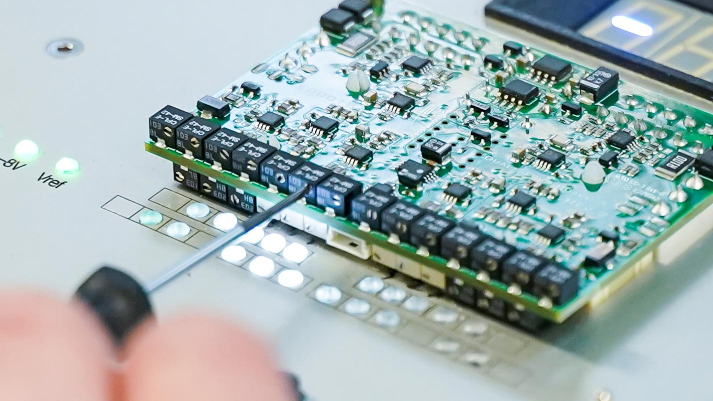
PCB cleaning - Fast, gentle cleaning of PCBs
PCBs are susceptible to many types of contamination, and so cleaning is an essential preparatory step in PCB manufacturing. This cleaning can be done in a variety of different ways. Laser cleaning is always an expedient option when a high degree of local control is deemed necessary. For example, lasers are used to clean manufacturing residues and dust from adhesive surfaces during the production of reversing cameras to ensure that the bonding material is highly adhesive. As Günter Lorenz, Director Business Development Laser Systems at ASYS Automation Systems, explains: “The benefit this process offers over conventional plasma cleaning is the significantly reduced risk of damage to the assembled electronic components. Bond pads, the small electrical connection points on the circuit boards, are cleaned by laser using a selective process that eliminates flux residues to optimise electrical transmission.” These points typically have a very small surface in the order of 2 mm x 2 mm, making them ideal for processing with lasers and laser components. Pulsed fibre lasers with a power of around 50 W are suitable as a laser source.
The scanner must meet equally high requirements in terms of accuracy – in the range of 15 μm. After all, neighboring components on the bond pad must not be destroyed. This means that the heat-affected zone must be kept as small as possible. This requires a high scanning speed, as offered, for example, by the RAYLASE SUPERSCAN-IV-15, to keep the cleaning process time as short as possible.
The SUPERSCAN-IV-15 digital, dynamic, versatile
The SUPERSCAN IV-15 is ideally suited to the cutting of PCB panels and the cleaning of bonding pads. The laser scanner’s model- based, digital regulation offers extremely dynamic responses and final speeds, which really come into play when used in surface ablation processes. The robust, water-cooled master block design minimises drift values.
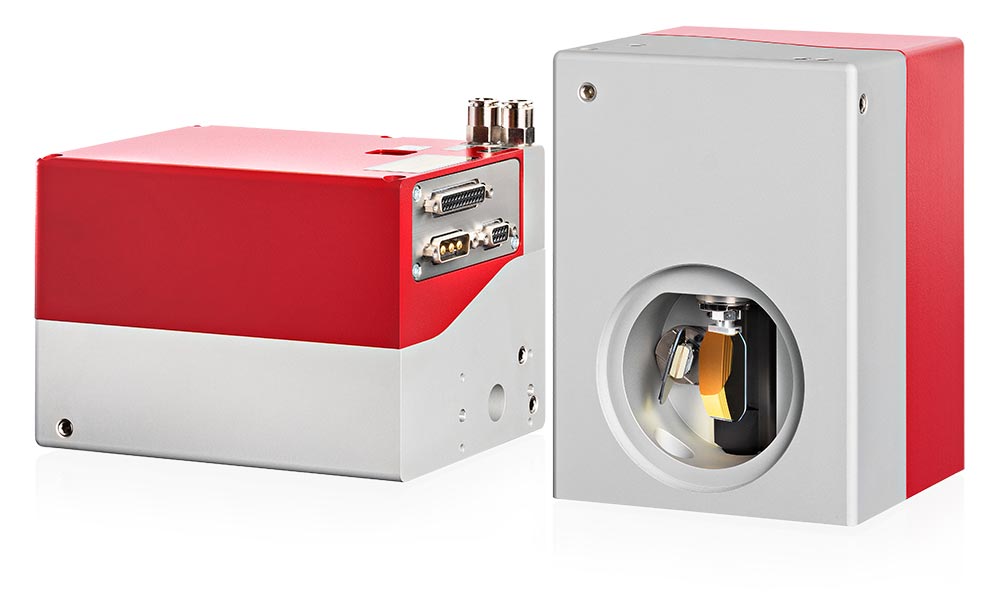
Special Features
- Control via the 20-bit SL2-100 protocol or
16-bit XY2-100 protocol - Greatly reduced power loss and minimal heat development thanks to a digital PWM output stage
- Highly dynamic responses and high speeds for maximum productivity, in particular for surface structuring applications
- Wide range of mirror substrates and coatings for diverse applications
- Available apertures (mm): 10, 15, 20, 30
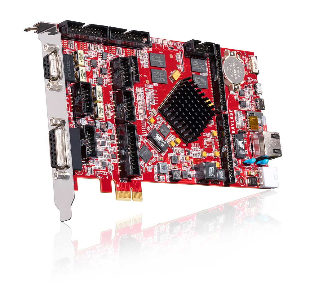
SP-ICE-3 control card
The SUPERSCAN-IV-15 could not exist without a control card. It is an integral part of the scanning system and the essential control unit for all laser processes. Flexibly configurable ports make the SP-ICE-3 control card suitable for universal use, even for very specific applications. Structuring applications can be implemented quickly thanks to the .NET programming environment and the flexibility of the SP-ICE-3 control card.
Your benefits
- Controls 2-, 3-, 4- and 5-axis deflection units as well as all standard laser sources
- Speed- and positioning-dependent laser power control
- Extended marking and processing on-the-fly (MOTF) functionality
- Can also be used as an external control card via Gigabit Ethernet
- Supports RL3-100 protocol
RAYGUIDE LASER PROCESSING SOFTWARE
RAYGUIDE software is highly innovative software developed by RAYLASE. It supports the setup of the galvanometer scanner, calibration of the working field and the creation and implementation of laser processing jobs. The following features are part of the ever-increasing portfolio of useful functions for the marking, cutting, cleaning and soldering of PCBs.
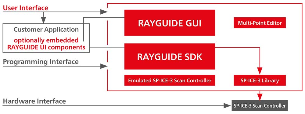
Your benefits
- User-friendly graphical interface or SDK programming (software developer kit)
- Embedded GUI and customer plug-ins possible
- Extensive functions for surface structuring
- Management of an unlimited number of control cards
To the product
LASER SOLDERING IN THE REFLOW PROCESS
This technique appears to offer particular benefits in cases where a very large number of soldered joints are located next to and overlapping one another. Laser soldering via scanner uses a re-flow process, which also shortens processing times. Two variants are available. In the first variant, the solder is already printed on the PCB and is then fused onto the corresponding point by the laser to connect the component with the conductive path. Alternatively, a dispenser is used to place the solder on the connection point, after which it is immediately soldered onto the point by laser. The scanner must meet the most rigorous requirements in terms of both precision and speed.

The MINISCAN-III-14 - digitally controlled, compact and robust
The MINISCAN III offers very stable digital control, which further improves noise and drift values, thereby making the system even more reliable and robust. Both the XY2-100 16 bit and the SL2-100 20 bit protocols can be used with the digital interface. A corresponding cable defines the use of the protocol. The MINISCAN corresponds to the more modest requirements for soldering and marking PCBs that apply in this case and offers a more cost-effective alternative to other techniques used in PCB manufacturing.
SP-ICE-1 control card
The SP-ICE-1 PCIe PRO control card offers high precision, flexibility and easy integration. The DLL driver software is included in the scope of the delivery. The integrated processor for real-time operation enables a precise synchronisation of scanner movement and laser control. Thanks to dual buffering, a second job can be downloaded while the first is still in progress. Used in conjunction with the MINISCAN models, this card is the ideal choice for marking and soldering PCBs.
To the product
Longstanding cooperation: ASYS Automatisierungssysteme GmbH
For 13 years, the ASYS Automatisierungssysteme GmbH based in Dornstadt, Germany, has been collaborating closely with RAYLASE GmbH. When Günter Lorenz, Director Business Development Laser Systems at ASYS, is himself amazed when he looks back over the history of the business relationship and realises the huge developments that have taken place up to this point: “Back in 2007, we were looking for an equal partner to collaborate with us on our own laser designs, and RAYLASE really impressed us on two counts.
The company was one of the most technically innovative in the market and the personalised support they provided was truly exceptional. ASYS successfully uses the SUPERSCAN IV- 15 and MINISCAN-III-14 from RAYLASE in our POLYPHOS DP laser depaneling, laser cleaning and laser marking product lines. We also use the SS-IV in our POLYPHOS SL laser soldering products.”
The current product portfolio of the ASYS Group covers more than 75% of a complete SMT product line, while also enhancing it with intelligent software and logistics solutions. ASYS is a leading provider of customised automation and holistic technology solutions, for example in the electronics, energy and life science sectors. “We’re delighted to be working with RAYLASE’s state-of-the-art solutions,” says Lorenz. ASYS has over 1,300 employees worldwide, with subsidies and business operations in more than 40 countries on five continents.
